

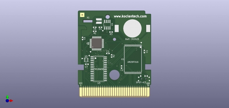
Reverse Engineering & PCB Designing

Service Description
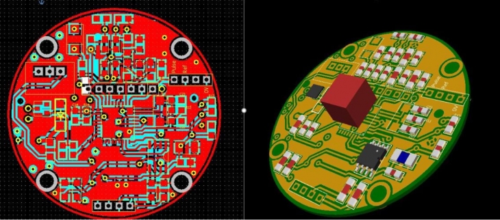
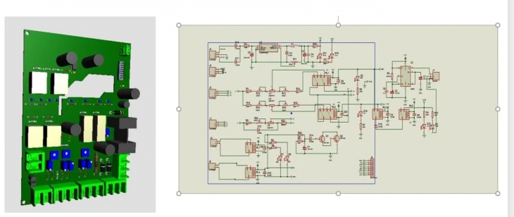
i have more then 4 years experience to design the Schematic, PCB layout, Reverse Engineering and 3D pcb layout through hole and SMD components.
PCB Designing Cover some points:
Single layer pcb (Through hole and SMD)
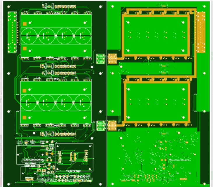
Double layer pcb (Through hole and SMD)
Multilayer pcb (Through hole and SMD)
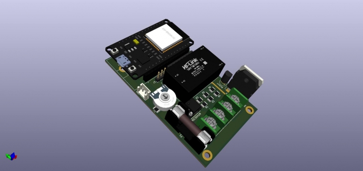
Power Supply (Through hole and SMD)
Arduino projects PCB
Technology Used
I use the KiCad, Altium designer, Proteus, Easy-PC PCB, EasyEDA softwares for pcb work
Frequently Asked Questions
What i Need FromYou for Reverse Engineering?
PCB images for reverse eingineering clearly and hd formate PCB dimensions through hole or SMD single layer or two layer reverse engineering images.
Do you perform a Design for Manufacturability (DFM) check of your designs?
yes, the DFM is necessary for final touch of PCB